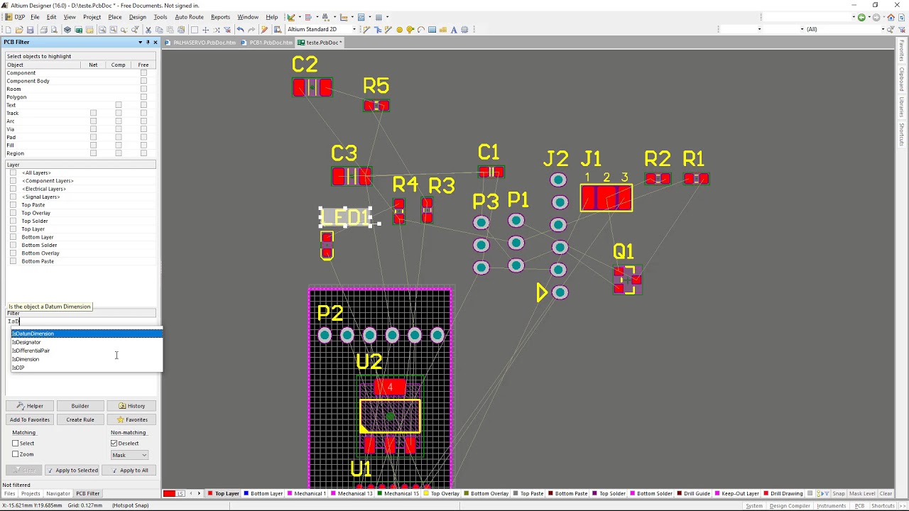
Altium designer tips #20: create keepout layer and board outline in Altium board designer changing sizes setting planning mode Altium designer change designators
Layout Guide to Changing Board Sizes in Altium Designer | PCB Design
[get 21+] schematic diagram network definition Altium : how to create board outline (robowild from the lab) Outline altium board create
Clearance altium board outline pcb documentation constraints designer
Altium designerLayout guide to changing board sizes in altium designer Layout guide to changing board sizes in altium designerBoard altium changing sizes designer outline redefine feature create using.
Managing design changes between the schematic & the pcb in altiumAltium pcb routing reverse managing changes howie modified Layout guide to changing board sizes in altium designerAltium designer board pcb changing sizes layout creating.

Layout guide to changing board sizes in altium designer
Altium designer 15.1Layout guide to changing board sizes in altium designer Altium outline boardAltium board changing sizes designer pcb editing outline moving corner while.
Board outline clearanceAltium layer keepout Board altium outline changing sizes designer modify notch feature create usingPcb altium schematic creare uno improves databases convert 3d.


Layout Guide to Changing Board Sizes in Altium Designer | PCB Design

Layout Guide to Changing Board Sizes in Altium Designer | PCB Design

Layout Guide to Changing Board Sizes in Altium Designer | PCB Design

Altium Designer Tips #20: Create Keepout Layer and Board Outline in

Layout Guide to Changing Board Sizes in Altium Designer | PCB Design
![[Get 21+] Schematic Diagram Network Definition](https://i2.wp.com/resources.altium.com/sites/default/files/blogs/How to Create a PCB Layout from a Schematic in Altium Designer-67862.jpg)
[Get 21+] Schematic Diagram Network Definition
Altium Designer - Tip#1 - How to change all designators properties

Board Outline Clearance | Altium Designer 16.0 User Manual | Documentation

Altium : How to Create board outline (RoboWild from the lab) - YouTube

Altium Designer 15.1 - Board Outline Clearance Check - YouTube
